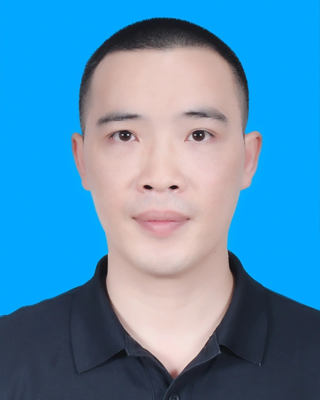
Personal Biography
I have long been engaged in the scalable growth of two-dimensional (2D) single-crystalline materials and their applications in quantum optoelectronics. My research focuses on the development of high-throughput equipment and CVD processes for the mass production of large-area, high-quality graphene films. This includes the annealing of industrial copper foils to achieve single-crystal Cu substrate, followed by the epitaxial growth of single-crystal graphene. Additionally, I investigate the photoelectron emission properties of various thin-film materials and the design of optoelectronic emitter structures.
Education Background
2012.09–2015.06 Sichuan University Engineering in Mechanical Manufacturing and Automation Master
2008.09–2012.06 Xihua University Engineering in Mechanical Design, Manufacturing and Automation B.S.
Working Experience
2022.08–Present Engineer, Shenzhen International Quantum Academy
2018.04–2022.07 Engineer, Southern University of Science and Technology
Representative Achievements
Invented Patent: Method for preparing single-crystal copper. (Granted, Patent No. ZL202110075702.6)
Invented Patent: Electron source, preparation method thereof, electron gun, and application thereof. (Appl. No. 2023118716710)
Invented Patent: Electron source, preparation method thereof, electron gun, and application thereof. (Appl. No. 2023118724280)