中文
中文
Quantized radio-frequency rectification in a kagome superconductor Josephson diode
Our quantum transport measurement platform integrates ultra-low temperature, vector magnetic field and low-noise electrical measurement capabilities to characterize quantum devices. The quantum devices are fabricated using micro-nano processing technology, which is compatible with the industry lithography technique. The millikelvin environment reduces the thermal noise to the quantum limit, enabling the emergence of quantum phenomena such as superconductivity and quantum Hall effect. The 3D vector magnet allows precise control of field orientation, essential for probing anisotropic magnetic responses. The low-noise electrical setup enables high-sensitivity detection of magnetoresistance or differential resistance of the devices. Besides, the microwave setup can irradiate sample to get excitation information under strong magnetic field. Together, these elements form a world-class facility for quantum transport studies. Our research areas include Josephson junctions based on topological materials, unconventional superconductors, and two-dimensional materials. The platform aims to uncover new physics in these quantum systems and develop possible applications through quantum devices.
The representative achievements done on the platform are shown as follows:
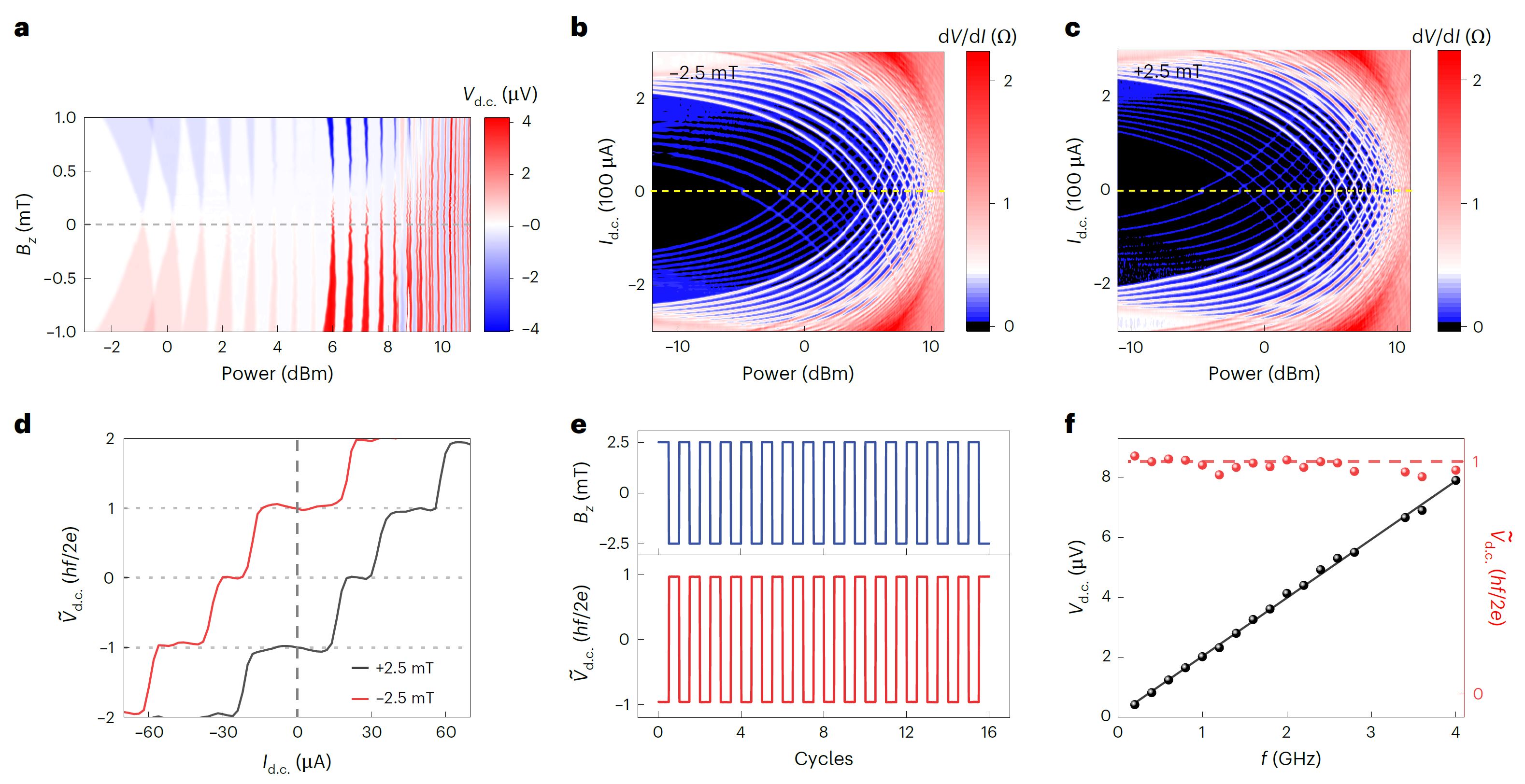
1. Quantized radio-frequency rectification in a kagome superconductor Josephson diode
Superconducting diodes promise low-dissipation rectification for superconducting electronics and low-temperature applications. Generating a quantized d.c. voltage from radio-frequency (rf) irradiation without external bias could enable self-powered cryogenic devices but are challenging to realize. Here we use the kagome superconductor CsV3Sb5 to demonstrate quantized rf rectification at zero magnetic field. Under rf irradiation without a current bias, a d.c. voltage emerges and scales linearly with the microwave frequency f as Vd.c. = hf/2e, where h is Planck’s constant and e is the electron charge. At constant frequency, the voltage increases in quantized steps with increasing rf power, consistent with the emergence of Shapiro steps. Our work establishes CsV3Sb5 as a potential platform for cryogenic-temperature wireless power sources and self-powered voltage standards. This work has been published on Nature Nanotechnology.
2. Broad and colossal edge supercurrent in Dirac semimetal Cd3As2 Josephson junctions
Edge supercurrent has attracted great interest recently due to its crucial role in achieving and manipulating topological superconducting states. Non- Hermitian skin effect, the aggregation of non-Bloch eigenstates at open boundaries, promises an abnormal edge channel. Here we report the observation of broad edge supercurrent in Dirac semimetal Cd3As2-based Josephson junctions. The as-grown Cd3As2 nanoplates are electron-doped by intrinsic defects, which enhance the non-Hermitian perturbations. The superconducting quantum interference indicates edge supercurrent with a width of ~1.6 μm and a magnitude of ~1 μA at 10 mK. The wide and large edge supercurrent is inaccessible for a conventional edge system and suggests the presence of non-Hermitian skin effect. The interplay between band topology and non-Hermiticity is beneficial for exploiting exotic topological matter. This work has been published on Nature Communications.